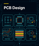
Functional Block Placement
PCB Design Workflow
Board Types and Construction
Design Constraints and Trade-offs
Component Selection and Datasheet Interpretation
Schematic Connectivity and Net Naming
Hierarchical Schematics and Design Reuse
Schematic Review and ERC
Schematic Symbols and Pin Mapping
PCB Footprints and Land Patterns
3D Models and Library Versioning
Board Outline, Keepouts and Mechanical Constraints
Layer Stackup and Materials
Copper Weight and Current Capacity
Controlled Impedance Planning
Decoupling and Clock Component Placement
Analog, Digital and Power Partitioning
Connector, Thermal and Mechanical Placement
Trace Width and Clearance
Via Types and Layer Transitions
Differential Pair Routing
Length Matching and Timing
BGA Escape and High-Density Routing
Ground Planes and Return Paths
Power Planes and Copper Pours
Grounding and Chassis Connections
High-Current Power Routing
Transmission Lines and Controlled Impedance
Reflections and Termination
Crosstalk and Impedance Discontinuities
PDN Impedance
Decoupling Network Design
DC Voltage Drop and Current Density
Plane Resonance and Antiresonance
EMI Sources and Coupling Paths
EMC-Oriented PCB Layout
Filtering, Shielding and Common-Mode Control
ESD and Transient Protection
Thermal Vias and Copper Spreading
Heat Sinks and Airflow
Thermal Derating and Hotspot Validation
Design Rules and Constraint Management
Design Rule Check (DRC)
Netlist and Connectivity Verification
Mechanical and 3D Clearance Verification
Design for Manufacturing (DFM)
Design for Assembly (DFA)
Solder Mask, Paste and Silkscreen
Gerber, ODB++ and IPC-2581 Outputs
BOM and Pick-and-Place Data
Design for Test and Test Points
Pre-Power Inspection and Safe Power-Up
Power Rail, Clock and Reset Validation
Signal Probing and Fault Isolation
KiCad
Altium Designer
PCB Version Control and Collaboration